
Research
Our mission Connecting phenomena across scales is a central challenge in computational materials science. Technologies rely on devices made from many materials working together. We develop and apply electronic structure theory methods to connect their atomic-scale physics with device-scale behavior, helping guide the design of sustainable electronic and photonic technologies, in close collaboration with experimentalists and industry.
Our methods Density-functional theory (DFT), many-body perturbation theory (GW), k·p perturbation theory, and AI/machine learning for discovering equations and effective models. We perform our calculations on the nation’s most powerful supercomputers.
Theme 01
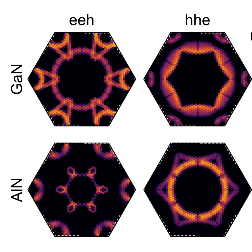
AI-driven discovery of effective theories for interacting electrons
The properties of materials emerge from how electrons interact with one another and with atomic nuclei. We use AI and machine learning to discover compact equations and effective theories that preserve the essential physics while making these calculations more tractable, allowing us to study more complex systems.
- Defects for quantum information sciences, electronics, and catalysis.
- Realistic interfaces for catalysis and electronic devices.
Example publications
- Electron correlation in semiconductors and insulators via symbolic regression
Physical Review B 114, 105112 (2026)
Theme 02
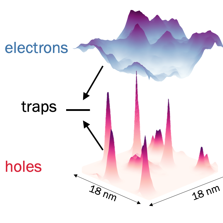
Designing disorder in materials for next-generation electronics
Disorder changes how electrons move, scatter, and recombine. We develop first-principles methods to predict these effects and understand when disorder limits performance or offers a way to control it.
- Semiconductor alloys for renewable-energy conversion.
- Amorphous oxides for next-generation electronics.
Example publications
- Increasing the mobility and power-electronics figure of merit of AlGaN with atomically thin AlN/GaN digital-alloy superlattices
Applied Physics Letters 121, 032105 (2022)
- High electron mobility of AlₓGa₁₋ₓN evaluated by unfolding the DFT band structure
Applied Physics Letters 117, 242105 (2020)
- Increased light-emission efficiency in disordered (In,Ga)N through the correlated reduction of recombination rates
Physical Review Applied 20, 064049 (2023)
Theme 03
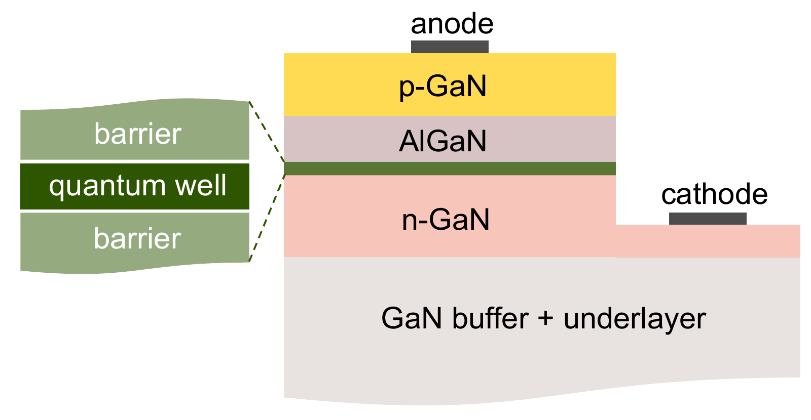
Connecting quantum chemistry with device physics
Devices contain several materials working together. Understanding them requires connecting the electronic properties of each material to processes across interfaces and throughout the device.
- Connecting ab initio simulations to TCAD electronic solvers.
- Designing device heterostructures for LEDs and next-generation AI hardware.
Example publications
- First-principles predictions of carrier mobility with record accuracy using GW perturbation theory
Physical Review Letters 137, 056303 (2026)
- Origin of the injection-dependent emission blueshift and linewidth broadening of III-nitride light-emitting diodes
AIP Advances 12, 125020 (2022)
- Enhancing light emission with electric fields in polar nitride semiconductors
ACS Photonics 12, 2902–2908 (2025)